




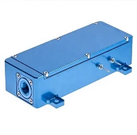
A common diode consists of a PN junction. A P-I-N diode is a PIN diode by adding a thin layer of low-doping Intrinsic semiconductor between the P and N semiconductor materials. Because of the existence of the Intrinsic layer, PIN diodes are widely used, from low frequency to high-frequency applications, mainly used in the RF field, as RF switches and RF protection circuits, and also used as photodiodes. PIN diode includes PIN photodiode and PIN switching diode. Take part 1.
3. PIN diode as RF switch
①Working principle
Because the RF resistance of the PIN diode is related to the DC bias current, it can be used as an RF switch and attenuator. Series RF switching circuit: when the diode is positively biased, it is switched on (short circuit); When the diode is zero-biased or reverse-biased, the bandwidth can be changed: not only the highest operating frequency of the switch will be limited, but also the lowest operating frequency will be limited, such as the PIN tube can not control the on-off of DC or low-frequency signals. The switch also has an upper operating frequency, which is affected by the cutoff frequency of the tube. The frequency band of the switch is required to be as wide as possible① because the frequency band of the signal source is getting wider and wider.
②Performance parameter
Insertion loss and isolation: Insertion attenuation is defined as the maximum available power P generated by the signal source.
The ratio of the actual power P to the load obtained when the switch is on, that is, P/P. If the actual power on the load when the switch is turned off is P, it represents the isolation, written in the form of decibels:

According to the definition of network scattering parameters, there are:
For the ideal switch: the attenuation is infinite when it is disconnected, the attenuation is zero when it is switched on, and the ratio of the two can generally only be required to be as large as possible. Since the impedance of the PIN tube can not be reduced to zero, nor can it be increased to infinite, the actual switch does not have infinite attenuation when it is disconnected, and it is not zero when it is switched on, generally only the ratio of the two should be as large as possible, the switch's on-off attenuation is called insertion loss, and the attenuation when it is disconnected is called isolation, insertion loss and isolation is a basic indicator of measuring the quality of the switch. The goal is to design switches with low insertion losses and high isolation.
Power capacity: The so-called power capacity of the switch refers to the maximum microwave power it can withstand. The power capacity of the PIN diode is mainly limited by the following two aspects: the maximum power consumption allowed when the tube is switched on; The maximum reverse voltage that the tube can withstand when it is cut off, that is, the reverse breakdown voltage. If the switch exceeds these limits when working, the former will cause the temperature in the tube to rise too high and burn; The latter will cause an avalanche breakdown in Zone I. It is determined by the smaller microwave signal power allowed in the on and off state of the switch. Nonlinear effects at high power (IIP3
It is also a major factor in the power of the switch, especially in mobile communication base stations.
Driver Requirements: The driver circuit of the PI N tube switch and the FET switch is different, the former needs to provide current bias, the latter requires bias, the driver is good or bad is one of the main factors affecting the switching speed.
Switching speed: refers to the speed of switching on and off, which is a very important indicator in fast devices. The current equation in zone I can be listed as follows:
The switching speed is increased to the order of ns, usually using a PIN tube with a very thin layer I, because the number of carriers stored in the thin layer I is small, and the switching time is greatly shortened, in this case, the switching time basically depends on the carrier crossing the I layer time, and has nothing to do with the carrier life. To improve the switching speed, the pipe with short carrier life can also be selected to increase the pulse amplitude of the control current, but the latter is limited by the maximum power of the PIN tube and the reverse breakdown voltage.
Voltage standing wave ratio (VSWR): Any component on the high-frequency signal channel will not only cause insertion loss but also cause an increase in standing waves on the signal transmission line. Standing waves are formed by the interference of transmitted and reflected electromagnetic waves, which is often caused by impedance mismatches in different parts of the system or impedance mismatches at connection points in the system.
Switching ratio: When a PIN tube does not consider the parasitic parameters of the package, its forward state can be expressed by the forward resistance R1, and the reverse state can be expressed by the reverse series resistance R2 and the I-layer capacitive reactance jXc, in series. Due to > R2, so the reverse state can be approximated by jXc, we call the ratio of positive and negative impedance of the two states Xc/R1 as the switching ratio, to measure the advantages and disadvantages of the PIN switch. If the switching ratio is to be increased, then C and R2 must be relatively small, and it can be seen that the switching performance decreases when the frequency is increased.
Contact information:
If you have any ideas, feel free to talk to us. No matter where our customers are and what our requirements are, we will follow our goal to provide our customers with high quality, low prices, and the best service.
 Email:info@loshield.com
 Tel:0086-18092277517
 Fax: 86-29-81323155
 Wechat:0086-18092277517


