



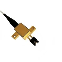
1. Semiconductor Lasers definition
We usually call the materials which have poor electric conductivity such as coal, artificial crystals, amber, and ceramic as insulators.
Metals that conduct electricity well, such as gold, silver, copper, iron, tin, and aluminum, are called conductors.
At room temperature, the conductive properties of materials between conductors and insulators are called semiconductors.
Compared with conductors and insulators, the discovery of semiconductor materials was relatively late, and it was not until the 1930s that the existence of semiconductors was truly recognized by the academic community when the purification techniques of materials were improved.

2. Development History
In 1833, the British scientist Faraday, the father of electronics, first found that the resistance of silver sulfide to a change in temperature is different from that of ordinary metals. Under normal circumstances, the resistance of metals increases with the increase in temperature, but Baradei found that the resistance of silver sulfide materials decreases with the increase in temperature. This is the first discovery of a semiconductor phenomenon.
In 1839, Becquerel of France discovered that a junction between a semiconductor and an electrolyte produces a voltage when exposed to light. This became known as the photovoltaic effect. It was the second characteristic of semiconductors that was discovered.
In 1873, Smith of England discovered the photoconductance effect of increasing the conductivity of selenium crystal materials under light, which is another characteristic of semiconductors. Although these four effects of semiconductors (the remnants of the Hall Effect -- the discovery of four associated effects) were discovered before 1880, the term semiconductor was first used by Coneyberg and Weiss probably in 1911. It was not until December 1947 that Bell LABS completed the characterization of the four properties of semiconductors.
In 1874, Braun in Germany observed that the conductance of some sulfide is related to the direction of the applied electric field, that is, its conduction is directional, and when a forward voltage is applied to both ends, it is conductive; If polarity of the voltage is reversed, it will not conduct electricity. This is the integral effect of the semiconductor and the third characteristic of the semiconductor. In the same year, Schuster also discovered the rectifier effect of copper and copper oxide.
Many people wonder why it has taken so long for semiconductors to be recognized. The main reason was that the materials were not pure. Without good materials, many materials-related problems are difficult to explain.
3. Semiconductor Lasers Classification
The chemical composition can be divided into element semiconductor and compound semiconductor two categories.
Germanium and silicon are commonly used as elemental semiconductors; Compound semiconductors include group Ⅲ and Ⅴ compounds (gallium arsenide, gallium phosphide, etc.), group Ⅱ and Ⅵ compounds (cadmium sulfide, zinc sulfide, etc.), oxides (manganese, chromium, iron, copper oxides), and solid solutions composed of group ⅲ-ⅴ compounds and group ⅱ-ⅵ compounds (gallium aluminum arsenic, gallium arsenic phosphorus, etc.).
According to their manufacturing technology, semiconductors can be classified into integrated circuit devices, discrete devices, photoelectric semiconductors, logistics, analogic, memory, and other categories. Generally speaking, these will be divided into small categories.

4. Characteristics of Semiconductor Lasers
Five characteristics of semiconductors: doping, thermal sensitivity, photosensitivity, negative resistivity temperature characteristics, and rectifier characteristics.
In a semiconductor forming a crystal structure, the electrical conductivity can be controlled by artificially adding specific impurity elements. Under the condition of light and heat radiation, its conductivity changes obviously.
5. Operating principle of Semiconductor Lasers
Intrinsic semiconductor: A semiconductor that contains no impurities and no lattice defects is called an intrinsic semiconductor. At extremely low temperatures, the valence band of the semiconductor is full band. After thermal excitation, part of the electrons in the valence band will cross the forbidden band and enter the empty band with higher energy. The conduction band becomes after the presence of electrons in the empty band, and the lack of an electron in the valence band forms a positively charged vacancy, which is called a hole.
Hole conduction is not actual motion, but an equivalent. When an electron conducts electricity, holes of equal charge move in the opposite direction. They generate directional motion under the action of an external electric field and form macroscopic current, which are called electron conduction and hole conduction respectively.
This type of hybrid conduction due to the generation of electron-hole pairs is called intrinsic conduction. The electrons in the conduction band will fall into the hole and the electron-hole pair will disappear, which is called recombination. The energy released during recombination becomes electromagnetic radiation (luminescence) or thermal vibration energy (heating) of the lattice. At a certain temperature, the generation and recombination of electron-hole pairs exist at the same time and reach dynamic equilibrium. At this time, the semiconductor has a certain carrier density and thus has a certain resistivity. As the temperature increases, more electron-hole pairs are generated, carrier density increases and resistivity decreases. Pure semiconductors without lattice defects have high resistivity and few practical applications.
Please go to Part 2 for more information
Contact information:
If you have any ideas, feel free to talk to us. No matter where our customers are and what our requirements are, we will follow our goal to provide our customers with high quality, low prices, and the best service.
 Email:info@loshield.com
 Tel:0086-18092277517
 Fax: 86-29-81323155
 Wechat:0086-18092277517


