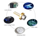
In the field of lithium battery manufacturing, laser technology has attracted much attention as the core supporting force of modern industry due to the urgent demand for high-precision and high-efficiency processing. Among them, the diode laser stack has emerged strongly due to its significant characteristics of high power and high stability, making it particularly suitable for the battery production process; Compared to other laser technologies such as fiber lasers and CO ₂ lasers, it exhibits unique differentiation advantages and is gradually becoming a key tool for promoting the upgrading of precision manufacturing of lithium batteries.

Technical principles
Core mechanism: Stimulated radiation effect based on semiconductor PN junction. When a forward current passes through, electrons and holes recombine in the junction region and release photons, which are reflected multiple times in the optical resonant cavity to form optical amplification. Finally, after breaking the threshold, a highly directional laser beam is output. The modern quantum well (QW) structure significantly reduces the threshold current to below 10mA, while increasing the output power to the hundred watt level.
Particle number reversal and gain medium: P-type and N-type semiconductor regions are formed by doping different impurities, and current injection achieves high-density distribution of charge carriers (particle number reversal), providing a basis for stimulated radiation. The gain medium is usually made of materials such as gallium arsenide or gallium nitride, and its band structure determines the wavelength characteristics of the laser.
Basic structure and working principle
Multi diode module integration and beam coupling technology: Multiple laser diode units are combined into a stacked structure through precise arrangement and optical coupling system to achieve power superposition. Using a mirror and lens system to spatially combine the light beams generated by each unit device, ensuring energy density concentration and mode quality control.
Wavelength selection and material absorption matching: Typical wavelengths such as 808nm, 940nm, etc. can be optimized and selected based on the spectral characteristics of the target material. For example, the high absorption rate of metal surfaces in specific infrared bands makes them suitable for welding or cutting processes; The coating of battery electrodes needs to be matched with corresponding wavelengths to achieve efficient processing. This customized design improves energy utilization and reduces the heat affected zone.
Key performance parameters
Power density and beam quality: High power density relies on multi module integration technology and efficient beam shaping schemes to ensure energy concentration at the focal point. The small beam divergence angle and pure mode ensure the focusing effect and processing accuracy after long-distance transmission.
Electro optic conversion efficiency: Thanks to advanced semiconductor materials and quantum well design, diode laser stacks have excellent electrical to optical energy conversion ratios, reducing energy consumption while minimizing thermal management difficulties.
Temperature control and long-term stability: The built-in heat sink structure and active cooling system effectively control the operating temperature, preventing wavelength drift or power attenuation caused by overheating. In addition, the packaging design takes into account earthquake resistance and anti-interference ability, ensuring stable performance even in complex industrial environments.
Core applications in battery manufacturing
1. Electrode processing
Polar cutting
Advantages: With high energy density and precise control, ultra narrow slits (micrometer level) can be achieved, significantly reducing the heat affected zone (HAZ) and avoiding material deformation or performance degradation; At the same time, it ensures extremely high edge flatness and no burrs, improving the subsequent assembly yield.
Process adaptability: Suitable for high-speed batch cutting of various positive and negative electrode materials such as ternary lithium and lithium iron phosphate, compatible with roll to roll automated production lines.
Extreme ear welding (breakthrough in the problem of copper/aluminum dissimilar metals)
Challenge: The significant difference in melting points between copper and aluminum can lead to the formation of brittle alloy layers and result in virtual welding.
Solution: Reliable connection with low defect rate between dissimilar metals can be achieved through wavelength optimization (such as near-infrared band), pulse waveform modulation, and dynamic shielding gas protection; Support multi-layer thin foil stacking welding, balancing strength and conductivity.
2. Battery assembly
Sealing welding of battery cell shell
Key requirement: High airtightness packaging without pores to prevent electrolyte leakage and external impurities from entering.
Technical highlight: Adopting high-speed scanning galvanometer combined with real-time closed-loop feedback system to ensure uniform and continuous welding seam; Supporting full cycle precision welding of materials such as aluminum alloy and stainless steel, with production efficiency more than three times that of traditional methods.
Busbar high reliability connection
Pain point of the scene: The stability of contact resistance under high current carrying is extremely high.
Innovative solution: Multi beam collaborative processing technology achieves multi-point synchronous welding, reducing stress concentration; Combined with online monitoring system for real-time detection of solder joint quality, the yield rate is greater than 99.9%.
3. Other value-added applications
Diaphragm micropore perforation
Functional upgrade: Processing of micrometer sized through-hole arrays with controllable diameters, precise control of electrolyte penetration paths, shortening ion transport distances, and improving charge and discharge efficiency.
Accuracy guarantee: Sub micron positioning accuracy avoids short circuit risks and adapts to the flexible processing requirements of composite diaphragm materials.
Permanent traceability identification
Industry compliance: High contrast surface engraved with QR codes/serial numbers, resistant to corrosion from cleaning agents and long-term cyclic aging; Support automated visual code reading integration to achieve full process traceability management.

Technological advantages and industry value
1, Efficiency and Cost Optimization
Ultra high electro-optical conversion efficiency (>50%)
Energy saving and cost reduction: Compared to traditional processing methods such as mechanical punching or resistance welding, its energy consumption is only 1/3 to 1/5 of the former, significantly reducing the electricity cost per unit of production capacity; Especially suitable for large-scale continuous production scenarios.
Advantages of thermal management: Low heat generation reduces the load on the cooling system, further reducing the investment cost of auxiliary equipment.
Modular architecture design
Rapid maintenance iteration: When a single diode unit fails, it can be replaced independently without the need to stop the line for maintenance of the entire equipment; Support power expansion and upgrade, adapt to the dynamic adjustment needs of production line capacity.
Controllable operation and maintenance costs: Standardized component supply shortens maintenance cycles, reduces spare parts inventory pressure, and overall lifecycle costs are more than 20% lower than fiber lasers.
2, Precision and Quality Innovation
Nanosecond narrow pulse width+Gaussian beam characteristics
Micro precision machining: The heat affected zone (HAZ) is controlled within ± 5 μ m to avoid electrode material oxidation/crystal phase change and ensure that the battery cycle life is not damaged; Suitable for safe cutting of extremely thin copper foil (<6 μ m).
Zero contact and stress free: Non contact processing eliminates mechanical indentation or dust pollution, and the yield rate is increased to 99.99%.
Closed loop intelligent control system
Dynamic compensation mechanism: Built in spectral analyzer monitors real-time output power fluctuations (accuracy ± 0.5%), automatically adjusts driving current to maintain process window stability; Combined with visual guidance algorithms, achieve adaptive correction of complex trajectories.
Data driven optimization: The cloud storage of process parameters is linked with AI learning models to continuously iterate the optimal formula library, reducing batch defects caused by human operational differences.
3, Empowering sustainable manufacturing
Green Production Paradigm
Zero consumables cycle mode: No consumables such as electrode rods or gas additives are required, and the waste only contains target material powder (recyclable and reusable); Compared to CO ₂ laser, it reduces several tons of greenhouse gas emissions annually.
Environmental compliance: No risk of harmful radiation leakage, electromagnetic interference (EMI) below the EU CE certification limit, meeting the cleanroom Class 100 requirements of the lithium battery industry.
Low carbon footprint throughout the entire lifecycle
Energy Efficiency Benchmark: From raw materials to disposal, carbon equivalent emissions are reduced by 40% to 60% compared to traditional processes, helping companies achieve ESG goals; Compatible with photovoltaic energy storage systems for power supply, promoting the transformation of factories towards "near zero carbon".
The diode laser stack, with its excellent electro-optical efficiency, precision machining capability, and green manufacturing characteristics, has become the core engine driving the improvement and efficiency of the lithium battery industry. It not only reconstructs the full chain process standard from electrode cutting to shell packaging, but also uses modular design and intelligent closed-loop control as a lever to help enterprises achieve low-cost and low-energy mass production. Facing the future, only by collaborating upstream and downstream of the industrial chain to tackle key technological bottlenecks such as material adaptability, beam shaping algorithms, and cross device interconnection, can we further unleash the revolutionary potential of this innovative tool and accelerate the transition of the new energy industry to the era of zero defect intelligent manufacturing.
Contact information:
If you have any ideas, feel free to talk to us. No matter where our customers are and what our requirements are, we will follow our goal to provide our customers with high quality, low prices, and the best service.
 Email:info@loshield.com
 Tel:0086-18092277517
![]() Fax: 86-29-81323155
Fax: 86-29-81323155
 Wechat:0086-18092277517


