



DPSS solid-state Lasers is a high-performance laser product, a new generation of solid-state laser with long life, low power consumption, high stability, high signal-to-noise ratio, high beam quality, and can be miniaturized and other advantages.
5. Quantum technology
The emerging field of quantum technology promises significant developments in various fields including metrology, cybersecurity, and computing. There are already many organizations that rely on atomic clocks to make the most accurate time measurements, and there is a massive movement to bring quantum gravimeters from the lab to the field to monitor the flow of magma in ice caps and volcanoes. Oil exploration companies have found a leak inside thousands of miles of pipelines running under the sea too costly for industry. GPS is now used every day in cars, mobile phones, or more recently in iot smart devices. But what happens if you enter a long tunnel, or want to dig deep underground? Current technology lacks the accuracy needed to help you navigate in this situation, but "Positioning, Navigation, and Timing" (PNT for short) is one of the key technologies being developed as quantum technology research advances.
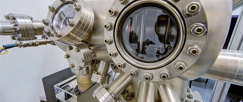
Quantum technology focuses on using precise and stable particles or atoms, and understanding the properties of these atoms helps us improve the accuracy of our measurements of time and space. In order to be able to interact with these atoms, they first need to be slowed down or "cooled" in order to examine them more thoroughly. For cooling atoms and examining them, highly coherent light is used, such as diode-pumped solid-state (DPSS) lasers. In quantum applications, the narrower the linewidth of the laser, the better the signal expected from the atom. It is also important to choose the wavelength associated with the atom to be captured. With the development and miniaturization of an optical dot clock, GPS accuracy below the millimeter level can be achieved. Due to the precision of these devices, they are also expected to be self-sustaining, without the need for continuous satellite communications. Quantum sensors are another branch of QT applications that have the potential to improve current gravity and magnetometry applications, both of which can be used to probe underground structures or even find objects in the deep ocean.
6. Fluorescence
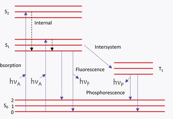
Photoluminescence is a general term that covers both fluorescence and phosphorescence. In the strictest sense, fluorescence is light emitted from the excitation to one of the singlet states within the material - usually very fast emission after excitation - while phosphorescence is light emitted from the triplet state - resulting in slower and more delayed light emission.
Photoluminescence is a form of luminescence - the emission of light by a material caused by absorbing energy - which in turn absorbs light energy, causing the material to emit at different wavelengths.
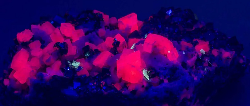
These terms are not usually used in this specific way, and generally fluorescence can be thought of as a rapid luminescence process after excitation, usually at or below the nanosecond level, in contrast to slower phosphorescence, which is usually considered at or above the microsecond level. While broadband light sources can produce a lot of photoluminescence, many applications require hyperspectral and spatial precision, such as confocal microscopy, crystal defect inspection, or dynamic mixtures of fluorescent dyes and fluorophores.
Many applications combine fluorescence with other measurements, such as Raman, where the ability of both techniques to use the same excitation source simplifies the integration and analysis of data. A typical example is solar cell manufacturing and research, where two techniques are used to analyze highly structured surfaces - for example, fluorescence to check inherent properties such as carrier lifetime or efficiency, and Raman microscopy to determine feature uniformity.
7. Optical tweezers
Also known as optical manipulation or optical capture, optical tweezers are a technique that allows the use of highly focused lasers to capture and move small particles. When the laser is focused on the particle, it undergoes a change in refractive index and slightly changes its direction of travel, moving along a gradient of electric field strength. This exerts the opposite force on the particle, and if the particle is smaller than the beam itself, causes it to be "trapped" in the center of the beam waist, where the electric field strength is greatest.
This has proven to be a very useful tool in many areas. Everything from individual atoms to custom tiny machines, and biological cells is being manipulated using this technology. Most biological samples are not damaged by NIR radiation (e.g. 1064 nm). As a result, scientists can now easily isolate individual bacteria and viruses for study without mechanical interference with them. The key to this technology is to obtain a "firm grip" on the particles, is excellent power and pointing stability, as well as excellent beam roundness, and low noise.
8. Photo etching
Lithography is the transfer of a designed pattern to a flat surface, either directly or through an intermediate medium - excluding surface areas where the pattern is not needed. In photomask lithography, the design is patterned onto the substrate and a laser is used to expose the pattern, allowing the deposited material to be etched away in preparation for further processing. This lithography method is widely used in the mass production of semiconductor chips.
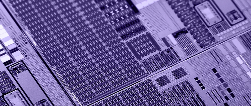
The ability to project sharp images of small features onto the chip is limited by the wavelength of light used. Current state-of-the-art lithography tools use deep ultraviolet (DUV) light, and these wavelengths will continue to span deep ultraviolet (193 nm), vacuum ultraviolet (157 nm and 122 nm), and far ultraviolet (47 nm and 13 nm) in the future. For the IC, MEMS, and biomedical markets, where demand for a wide range of features and substrate sizes is growing, complex products and frequent design changes drive up the cost of manufacturing these highly customized solutions at lower volumes. Traditional photomask (photomask) -based lithography solutions are neither economical nor practical for many of these applications, where the cost and time required to design and manufacture a large number of mask sets can add up rapidly.
However, maskless lithography applications are not affected by the very short ultraviolet wavelength requirements, instead using lasers in the blue and ultraviolet ranges. In maskless lithography, the laser creates microns and nanostructures directly on the surface of the photosensitive material. This general lithography method does not rely on mask consumables and can make layout changes quickly. As a result, rapid prototyping and development become easier, with the advantage of having greater design flexibility while maintaining large area coverage (such as 300 mm semiconductor wafers, flat panel displays, or PCBS).
To meet the needs of rapid production, maskless lithography lasers have characteristics similar to those used in photomask applications:
Continuous wave sources with long-term power and wavelength stability and narrow line widths mean less variation in the mask signature.
Long-life stability with little to no maintenance or disruption to production cycles is important for both applications.
DPSS lasers with ultra-stable narrow linewidth, wavelength stability, and power stability are well suited for both lithography methods.
Contact information:
If you have any ideas, feel free to talk to us. No matter where our customers are and what our requirements are, we will follow our goal to provide our customers with high quality, low prices, and the best service.
 Email:info@loshield.com
 Tel:0086-18092277517
 Fax: 86-29-81323155
 Wechat:0086-18092277517


