


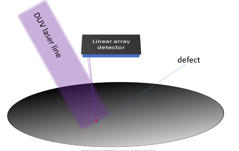
In the semiconductor industry, extremely small surface defects and particles are a major problem, which can reduce yields and consume the time and cost of production. Therefore, detecting defects and contamination on semiconductor wafer surfaces is critical, a challenge faced by many customers in the semiconductor metrology industry. One of the fast and cost-effective methods for wafer surface inspection is to use laser line illumination and dark/bright field microscopy to detect defects, typically below 100nm at deep ultraviolet (DUV) wavelengths. In this method, Holoor shows that when the line is scanned radially, the wafer rotates, creating a large sampling area of the wafer, which can reduce the scanning time. Since most ultraviolet and deep ultraviolet lasers do not have a line output profile, a line laser element is often used to shape the laser into a line shape.
Requirements for the use of line laser optical elements in semiconductor wafer inspection
The requirements for wafer defect detection using laser lines at deep ultraviolet wavelengths are very strict - often they must be very long lines ( >10mm), while maintaining the laser line. 10um narrow width and excellent uniformity. For dark field microscopy, the laser line needs to be projected onto the wafer at a grazing Angle while remaining tightly focused over a very long line length. Such lines cannot usually be achieved by a single diffracted optical element, such as a linear homogenizer, because they produce speckles on a single-mode laser, while a multimode laser cannot focus to a tight line at a reasonable depth of focus.
This type of performance requires Holoor's high-precision beam-shaping optics to generate laser lines with the desired edge clarity, uniformity, width, and length. This precision can often be achieved by diffractive optics or free-form optics.
Beam shaping method for wafer defect detection
The stringent requirements for linear laser modules indicate that there are several possible solutions to the challenges of beam shaping, all of which require diffractive or free-form refraction optics systems with multicomponent components.
For typical cases with line lengths in the 10-20mm range, a single-mode deep ultraviolet laser provides sufficient power for detection. This situation requires multiple element flat-top beam shaping, where the first element produces lines and the last element in the system is similar to a diffractive optical lens, used to collimate the lines and focus them on the fast and slow axes. For very long lines, it is usually >50mm, single-mode DUV lasers rarely have high laser power. Therefore, a multimode laser must be used, requiring an M2 transform to focus to the narrow line. This can be achieved by combining diffraction solutions such as Leanline with line homogenizers to produce good uniformity. Laser beam splitters diffractive optical elements can be used to generate focal lines with the same intensity. The line is used to scan along a radial path in the wafer, enabling high-resolution defect detection at lower laser power. This comes at the cost of slowing down the scanning speed, since the area imaged at any given time is significantly smaller.
Advantages when used as a key shaping element in in-line laser elements Diffractive optics offer several key advantages in shaping a laser into a line (or lines) for demanding applications such as wafer metering:
1. Diffractive optical elements have almost absolute angular accuracy - this is crucial when precise distances need to be measured, such as in precision metrology applications.
2. Diffractive optical elements have a high LDT (damage threshold), and Doe optical elements are usually flat elements, so they can be directly integrated into multi-component systems.
3.DOE optical elements can combine multiple functions on a single surface. For example, a laser line splitter can be used in combination with a line diffuser to generate multiple lines, enabling multi-channel defect detection (allowing pixels in a linear detector to "rest" without deep ultraviolet illumination).
4. Laser beam shaping optics based on diffractive optical elements have very low thermal sensitivity, almost no thermal lens, even a slight defocus will damage performance, so it is particularly suitable for narrow laser line shaping.
Question and Answer:
1. How can line laser components be used for wafer defect detection?
In wafer inspection, deep ultraviolet beams or spot lines are used as illumination sources to achieve resolution. 100nm high resolution bright or dark field microscopy. The line is generated by a line laser element or a laser line splitter.
2. What are the challenges of laser line shaping in wafer inspection?
Metrological applications such as wafer defect detection require long axis (>10mm) very uniform strength, while usually required. 10um narrow line to maintain high defect detection resolution. Sharp edges are also required, and in dark field microscopy, the lines also need to be projected at a high grazing Angle while still maintaining their tight focus.
3. Which beam shaping methods are used for wafer defect detection?
A typical linear spot is a multicomponent system that produces a flat-topped, collimated narrow line focused on the surface. Alternatively, a laser splitter can produce a line of light that can then be scanned radially while rotating the wafer. Longer lines require higher laser power, which can only be achieved with multi-mode lasers. Therefore, the optical element of a laser line generator usually includes an M2 conversion component that allows the line to be tightly focused on one axis while making it more uniform on the second axis, followed by a line levelling sheet and a focusing optical element.
4. What are the advantages of diffractive optical components to linear laser modules?
The diffraction line laser module provides almost absolute angular accuracy, a key parameter needed to stabilize the metrology process. They also have flat, high damage thresholds, and the ability to integrate multiple optics on a single surface, making them ideal for multicomponent systems operating with high-power DUVs.
Contact information:
If you have any ideas, feel free to talk to us. No matter where our customers are and what our requirements are, we will follow our goal to provide our customers with high quality, low prices, and the best service.
 Email:info@loshield.com
 Tel:0086-18092277517
 Fax: 86-29-81323155
 Wechat:0086-18092277517


