



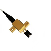
High-power Semiconductor Lasers are widely used in intelligent manufacturing, laser communication, laser sensing, medical beauty, etc. Since their birth, they have made great progress in theory, practice and application, accounting for most of the overall laser market. Among them, high-power semiconductor lasers in the near-infrared band are the best.
Near-infrared high-power semiconductor laser chips High-power semiconductor laser chips are the core light sources of contemporary high-energy lasers represented by optical fiber, solid-state and direct semiconductor lasers. The power, brightness, and reliability of the laser chip are core indicators, which directly affect the performance and cost of the laser system.

The main structure of a semiconductor laser chip includes an epitaxial light-emitting layer that provides a laser gain medium, an electrode that injects carriers into the epitaxial light-emitting layer, and a cleavage cavity surface that forms a resonant cavity. The development process of the chip includes the steps of epitaxial structure design and material growth, chip structure design and preparation process, cavity surface cleavage passivation treatment and optical coating, chip packaging test, chip life reliability and performance analysis, among which the core indicators directly affect The three key technologies are epitaxial structure design and material growth, chip structure design and preparation process, cavity surface cleavage and passivation treatment.
(1) Epitaxial structure design and material growth Epitaxial structure design and material growth involve the gain and pumping of the laser, which directly affects the electro-optic efficiency of the chip. The main factors are heterojunction and bulk material voltage loss, carrier leakage loss and light absorption loss . According to the energy band analysis of semiconductor materials, the heterojunction voltage mainly comes from the interface between the confinement layer, the substrate and the waveguide layer, and the heterojunction voltage of the chip is effectively reduced through interface gradient and high doping optimization. Bulk material resistance can be achieved by adjusting material composition to increase carrier mobility and increasing doping concentration. Reducing the carrier leakage loss requires sufficient carrier confinement barrier, especially the p-plane electron barrier. Therefore, the reduction of bulk material resistance and the improvement of carrier confinement need to be considered comprehensively to optimize the material composition. Optical absorption loss can usually be achieved by designing an asymmetric ultra-large optical cavity waveguide structure. When the total thickness of the waveguide layer remains unchanged, the thickness of the p-plane waveguide layer is reduced and the thickness of the n-plane waveguide layer is increased, so that the main part of the optical field is distributed in the low Absorb the low-resistance n-plane, reduce the overlap of the optical field and the high-absorption p-plane, reduce the voltage of the bulk material, and reduce the light absorption loss. At the same time, combined with the gradual doping distribution design, the simultaneous optimization of bulk material voltage loss and light absorption loss is realized. Laser chips in the 900 nm band usually use InGaAs quantum wells as the gain material, and AlInGaAs quantum wells with high strain to increase the gain, but AlInGaAs quantum wells as a quaternary material have stricter requirements for material growth control. It is necessary to optimize the atmosphere ratio and growth temperature rate to increase the nucleation energy of quantum well body defects, thereby reducing the defect density of quantum wells and growing high-quality and high-strain quantum wells.
(2) When the chip structure design and fabrication process work in high-power mode, the lateral high-order mode intensity of the chip increases, resulting in a sharp increase in divergence angle and a decrease in brightness. Absorption and scattering at the edge of the waveguide are generally used in literature reports to reduce the intensity of high-order modes, but this will also cause additional absorption loss to low-order modes and reduce the total optical power. In addition, when working at high power, the optical field intensity of the chip is unevenly distributed in the longitudinal direction, while the carrier concentration generated by the current injection of the conventional structure chip is uniform in the longitudinal direction, so the optical field intensity and carrier concentration distribution cannot be Matching, this will produce a vertical space hole burning effect, resulting in power saturation. One way to solve this problem is to adjust the device structure of carrier injection distribution.
(3) Cavity surface cleavage and passivation treatment The main failure mode of high-power semiconductor laser chips is cavity surface optical catastrophe damage (COMD). COMD comes from the light absorption of the cleaving cavity surface and the surrounding area when the chip is working at high power. Surface light absorption is caused by cleavage of surface dangling bonds, surface oxidation and surface contamination, while conventional cavity surface cleavage is carried out in the atmosphere or low vacuum environment, and this problem cannot be avoided. The light absorption in the region near the cleavage surface comes from interband absorption. When the chip works at high power, the temperature of this region increases, resulting in a decrease in the band gap of the material and an increase in interband absorption. The most effective way to reduce this type of absorption is to form a wide band gap (low absorption ) window structure. Through the development of epitaxial structure design and material growth, chip structure design and preparation process, cavity surface cleavage and passivation treatment, Suzhou Everbright Huaxin Optoelectronics Technology Co., Ltd. (hereinafter referred to as "Everbright Huaxin") has launched a 28 W semiconductor laser chip. The power increase of the chip mainly comes from the optimized design of the chip epitaxial structure and the improvement of the special processing technology of the cavity surface. The output power of semiconductor lasers is mainly affected by factors such as laser threshold, slope, and high current power bending. Usually by reducing the doping concentration of the pn junction to achieve the reduction of the threshold and the increase of the slope, and too low doping concentration will lead to the increase of the resistance of the pn junction and the increase of the chip voltage. In order to solve the problem of optimizing the balance between threshold slope and voltage, Changguang Huaxin optimized the thickness of the waveguide layer of the asymmetric large optical cavity structure, and carefully designed the distribution of doping concentration in different regions of the pn junction, so as to reduce the threshold and improve the slope efficiency. The effect of keeping the voltage basically constant. High current bending is mainly due to the decrease of internal quantum efficiency when high current is injected. Everbright optimized the energy band structure of the material near the gain region of the laser structure, improved the confinement ability of pn junction injected electrons, and effectively enhanced the quantum efficiency during high current injection. While optimizing the power of the laser chip, Everbright continues to improve the material quality of the special treatment process of the cavity surface to reduce the defect ratio, improve the ability of the cavity surface to resist optical catastrophe damage, and ensure that the 28 W high-power laser chip meets the requirements of the industrial market for laser life. requirements.

As a practical tool, the near-infrared high-power semiconductor light source module fiber laser has developed rapidly in recent years due to its unique advantages, and plays an important role in the fields of industrial manufacturing, processing and scientific research. As the core upstream device of the fiber laser, the development of the pumping source also accompanies and even promotes the development and progress of the overall technology of the fiber laser.
(1) Industrial fiber laser pumping source In recent years, the industrial fiber laser market has developed rapidly and has a strong momentum. Fiber lasers have taken the lead in the industrial laser processing market with their unique technology and application advantages. As far as the industrial fiber laser market is concerned, the low-to-medium power fiber laser technology has matured and stabilized, and has fully entered the stage of cost competition.
2) Fiber laser pumping source for scientific research. Fiber lasers for scientific research generally have higher requirements on brightness or are used in some special application scenarios. These requirements extend to the pumping source. Generally, the pumping source is required to have high brightness and small size. , lightweight, wavelength locking and other characteristics. Small volume requires compact packaging design for the pumping source, and light weight requires necessary weight reduction treatment for the pumping source and the use of new low-density metal materials to process the tube shell on the basis of ensuring heat conduction efficiency.

High-brightness kilowatt-class fiber-coupled direct semiconductor lasers High-brightness kilowatt-class fiber-coupled direct semiconductor lasers have the characteristics of high brightness, wide wavelength range, high electro-optical conversion efficiency and easy use, and have a wide range of potential applications in industry and scientific research fields, such as for Metal material processing, Yb-doped fiber laser pumping, Raman nonlinear fiber laser pumping, and energy transfer. Brightness is defined as B=P·A-1·Ω-1, where P is the output power of the laser, A is the area of the beam waist of the output beam of the laser, and Ω is the solid angle of the divergence angle of the output beam of the laser. Generally speaking, the higher the brightness, the smaller the focused spot size and the longer the working distance. The continuous output power of a single laser diode light-emitting unit (or laser diode single tube) is less than 40 W, and it is necessary to use different beam combining methods to combine dozens to hundreds of single tube chips into a beam output to achieve kilowatt-level output. Conventional direct semiconductor lasers are based on a laser diode single tube or bar (composed of multiple single tubes), using spatial beam combining, polarization beam combining, coarse spectrum beam combining or fiber beam combining to increase output power. Direct semiconductor lasers based on this type of beam combining technology have high output power and low cost, and are favored by the industry, and can be used for welding and cladding of metal materials. Using the dense spectral beam combining technology based on a single-tube chip, Everbright Huaxin has successfully developed a variety of high-brightness fiber-coupled direct semiconductor lasers, which greatly improved the output brightness of direct semiconductor lasers (> 200 MW cm-2 Sr-1) and Electro-optical conversion efficiency (> 45%). For example, in 2019, Everbright launched a 1 kW, 220 μm/NA0.22 semiconductor laser (with an output brightness of 21MW cm-2 Sr-1), which has been widely used in thin plate welding; in the same year, it launched a 4 kW, 600 μm /NA0.22 (output brightness of 11 MW cm-2 Sr-1) direct semiconductor laser has been widely used in surface cladding. However, due to the large core diameter of the output fiber and low brightness, this type of laser cannot be used for cutting metal materials and scientific research applications that require high brightness. Figure 8 shows the simulation results of multiple single-tube chips spatially combining fiber coupling. The maximum number of single-tube chips accommodated by a 100 μm/NA0.22 fiber is 12, so the output power is only 12 times that of a single single-tube chip.
Near-infrared high-power semiconductor lasers can be used as pumping sources and core devices for solid-state and fiber lasers, and can also be directly used in industrial and scientific research fields through different beam combining technologies, occupying a large market in the laser industry. The single-tube chip is a unit device of a high-power semiconductor laser pumping source. Its comprehensive characteristics determine the output optical power, conversion efficiency, and volume of the final pumping source module. Therefore, it has become the focus of our research and development and research. With the in-depth theoretical research of the research team, the progress of material growth technology, and the development of packaging technology, JTBYShield has greatly improved the output power, life, reliability, and application practice of high-power semiconductor lasers, greatly shortening the time between foreign gap. In the future, we will not only make breakthroughs in key technologies, but also achieve industrialization, and realize the full localization and industrialization of high-end laser pumping source chips and devices.
Contact information:
If you have any ideas, feel free to talk to us. No matter where our customers are and what our requirements are, we will follow our goal to provide our customers with high quality, low prices, and the best service.
 Email:info@loshield.com
 Tel:0086-18092277517
 Fax: 86-29-81323155
 Wechat:0086-18092277517


